PCB Design: A guide for beginners
PCB design is an art form that’s been refined considerably over the years. Every circuit design will go through several different phases over the course of its development: from early prototypes to the finished product. If you’re confident in your skills, you might move through these phases very quickly – but the overwhelming majority of electronic circuit projects will follow the same development path.
However you decide to approach your design process, the principles remain the same. The early versions of your circuit will be large and unwieldy, but easily reconfigured whenever inspiration strikes. The later versions, by contrast, will be smaller, lighter and more elegant, but their components and connections will be fixed into place. As your PCB design is gradually refined, you’ll be able to move from the former to the latter.
Let’s take a look at how a circuit design moves from an idea in the designer’s head to a real, physical product that’s ready to be deployed commercially.
The first version of a given circuit will almost always be built using a prototyping device called a breadboard. This is a small piece of plastic covered in a grid of tiny holes. Inside is an arrangement of metal strips, which connect components placed into the holes above. Designers who are in this early stage of development are said to be ‘breadboarding’ their projects.
Most breadboards are arranged into two groups of five-pin columns. Running down the sides are rows of interconnected pins which typically function as +5v and ground. The middle ground between the two sets of columns is spaced so that a DIP integrated circuit can mount the top, with pins on either side. This is where your microcontroller might sit, forming the heart of a flexible electronic circuit circuit. At this stage, however, you’ll probably be using an Arduino or something similar.

The layout of a breadboard allows components to be connected to one another via the columns and rows. For example, you might have a resistor running from one column to another, which in turn is connected to an LED. Either end of the circuit could then be connected to the two power terminals.
Breadboards can be reconfigured extremely quickly. This means that when inspiration strikes, the designer can make changes and observe results within seconds. As such, breadboarding is a great way to refine a rough idea into a workable circuit. You might, for instance, swap out resistors or capacitors for those of different values and see what happens. However carefully you’ve calculated the values ahead of time, it’ll take a real-world electronic circuit to put the theory to the test.
Using a breadboard means you won’t need to mess around with soldering irons. This will help keep your workstation free from scorch-marks, spattered solder and blackened sponges.
Since it doesn’t require the wielding of any red-hot implements, breadboarding is a safe way to get your circuit functioning. It’s therefore also suitable for small children and complete novices. Soldering is a basic skill for an engineer, but that doesn’t mean we need to use it at every opportunity.
Breadboards are not expensive; they usually cost a just a few dollars. You’ll also be able to streamline the design process by eliminating the costs associated with soldering and printing multiple circuit boards at this early stage of development.
Once you get the hang of how a breadboard is arranged, you’ll be able to quickly form a deeper understanding of what your electronic circuit does and how it can be changed. This makes breadboarding a fantastic way to familiarize yourself with your components and how they interact.
So why do we bother with printed circuit boards at all? Well, if you’ve spent even a small amount of time with your breadboard, the answers will seem obvious.
When you create a breadboard, you’re not actually attaching components to one another. The only thing keeping the connections intact is gravity. This makes the use of breadboards in the real world impracticable. While it might be possible, say, to construct a remote controller for your television using a breadboard, the thing would disintegrate after being thrown onto the sofa a few times. If you don’t believe us, try lifting your breadboard prototype over your head and giving it a shake!
There’s another reason that you wouldn’t want to use a breadboarded remote controller; it would be absolutely massive. Breadboards use DIP components rather than smaller surface-mounted ones. They can’t be squeezed closer together than the grid allows. And having loops of cabling sprouting up everywhere will enormously increase the size of the circuit. Add to this the fact that you can’t reduce the footprint of a breadboard without taking a hacksaw to it, and it becomes clear that a breadboarded circuit will necessarily be significantly larger than a printed one.
In conclusion, as useful as breadboards might be, they’re the starting point of an electronic circuit rather than its final form. If you want your circuit to be ready for market (or even repeated personal use) you’ll need something to create a printed circuit.
Once your PCB design is ready, you can start preparing to create a fixed circuit board. PCB manufacturers will want more than a vague idea of how you’d like your circuit to look, therefore you’ll need to provide concrete and precise instructions.
Even if you don’t intend to work with outside parties, you’ll make life significantly more comfortable by settling on a final board layout at this stage.
With so many components to choose from, you might wonder which will make the best match for your PCB design. Let’s consider a few factors that might influence your decisions.
You’ll naturally want to minimize the cost of your circuit by selecting the cheapest available parts. If you’ve got hundreds of resistors, capacitors and LEDs crammed onto each circuit board, a difference of just a few cents can be significant.
Some components are smaller than others. If you want to make your circuit as small as possible, you’ll want to dispense with drilled-hole components and go instead for smaller SMD (that's surface-mount device) alternatives. This will in turn allow you to shrink your circuit board and eliminate unnecessary drilling, both of which will help to minimize costs.
Surface-mounted components are significantly smaller. You might suppose that this therefore means that they’re more difficult to hand-solder, and you’d be right. But if you know what you’re doing, you can deal with them without the need for specialized ‘precision’ tips. There are some excellent instructional videos out there on YouTube, most notably from Dave Jones’s EEVblog. The more you practice, the better you’ll become.
On the other hand, since you’ve been working with DIP components up until this point, you might feel more comfortable sticking with them. For one-off projects with just a few components, the savings you make by making the switch to surface mount might not justify the hassle.
Once you’ve selected your components, you’ll need to describe how they should connect to one another. This is done in a very specific way, using a schematic that can be understood by any qualified engineer. They differ from a breadboard in that they’re a description of the electronic circuit rather than the circuit itself. Can you imagine looking at a messy breadboard and attempting to work backwards to figure out all the connections? The process would take hours – or even longer. A good circuit schematic eliminates this extra work, creating a diagram of the circuit that can be referred to at any time.
You’ll need to learn to read and create schematics if you want to be able to communicate your ideas to others (and indeed, to analyse them yourself). Circuit schematics use a range of symbols to represent components, and straight lines to connect them. These lines can only bend at right-angles, which results in a clean, comprehensible illustration.
The software that allows you to create your schematic will often also design your PCB for you. The automatically-generated PCB layouts might be a little less than perfect, but once you’re familiar with the programs, you’ll be able to dive in and make the necessary optimizations.
Let’s run through a few basic symbols:

Note that some of these symbols will vary according to where in the world you are. Americans might represent a resistor using a zig-zag, while everyone else draws a rectangle. Moreover, these symbols can be varied to represent different sorts of components; drawing a line through a resistor, for example, makes it a variable resistor.
When you’re first coming up with your PCB design, you might elect to hand-draw your schematic. But eventually you’ll need to create a digital version that can be easily altered and made ready for a printed circuit board. That means using one of several popular pieces of circuit-design software.
The precise method you’ll use to create your circuit will vary according to the software you’re using. Let’s take a look at EAGLE, one of the more popular options.
Once you’ve installed the program and created a new blank project, you’ll need to import your components into EAGLE. This can be done using the “add components” button on the left-hand panel, which will bring up an enormous list of components from various manufacturers.

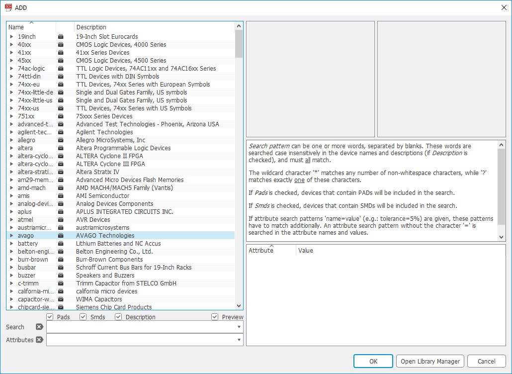
At first, this can be a little bewildering; but given that there are so many different types of components available, it’s necessary. Using the search function, you’ll be able to pinpoint exactly the component you’re looking for. Each component in Eagle comprises three elements:
You’ll see a preview of the component’s symbol on the design, and how it’ll look when it’s on the board itself. Be sure that you’ve selected the right version of the component if you want the final slot on the PCB to be the right size. When you get a little more advanced, you’ll be able to create your own custom components – that way you can be sure that you’re following precisely the dimensions laid out in each component’s datasheet.
Once you have all of the components of your project, you’ll need to connect them. This can be done using the wire or net tools. The ‘net’ tool is preferable unless you’re fine-tuning the schematic right at the end of the design process.

Once you’ve gotten your circuit design finalized in EAGLE, you can use it to generate a PCB. This will contain all of the footprints of your design, specify where the components are placed, and define the printed wiring which will adjoin them. Generate the printed circuit board by pressing the ‘SCH/BRD’ button at the top (or by hitting File>Switch to Board).
After the board is generated, you’ll need to drag the footprints of your components onto the board. From there, you can connect them either manually, or by using the ‘auto route’ function. Simply click on the yellow lines that represent connections using the ‘route’ tool, and join everything up. You’ll find comprehensive instructions on routing versus auto-routing on Autodesk’s website.
If you’re going to get your circuit professionally printed by a specialist manufacturer, you’ll need to turn it into something called a Gerber file. This contains the board-layout instructions that a fabrication plant will need to create the PCB, including drilled-hole locations, the printed wiring layout and where your components will go. From your PCB layout in Eagle, you can create a Gerber file by pressing the ‘CAM’ button on the toolbar. From there, select File>Open>Job.
From the resulting popup, you can specify exactly what information is going to go to the Gerber file, including multiple silkscreens. If your PCB includes holes to be drilled, be sure that you’ve detailed these in a separate Gerber file.
Now you’re ready to create the PCB. This can be done in one of two ways:
There are two popular methods to create your circuit board at home:
This involves printing your PCB design onto a piece of glossy paper (of the sort you might get from a magazine). You can then transfer the design to your circuit board using an iron. This is your mask, which will protect certain areas of the board from the etching solution you’ll use to remove most of the copper. Let’s run through the process, step-by step:
Use a laser printer to print a mirrored version of your circuit board layout, ensuring that the printout goes onto the shiny side of the paper. Ensure that the output is black.
Next, you need to take a copper board and saw it to the appropriate size. This can be done using a hacksaw, band-saw or circular cutter. Once it’s the right size, sand away the topmost layer of copper using steel wool. This layer protects the underlying copper while it’s in transit.
Place your PCB design face-down onto the copper. Use tape to secure it into position. You can either use a permanent marker to trace over your circuit, or you can use an iron to fuse the toner (the stuff that makes your print) onto the copper. Do this by placing the board onto a clean table that’s protected by a cloth (one you don’t mind burning).
Keep everything steady using pliers while you apply the iron. Around ten seconds of pressure will stick the two together temporarily. Next, flatten the iron against the board for around five to ten minutes. When you’re done, the ink will have transferred. Do not leave the iron unattended while this is going on, and do not touch the copper plate while it’s still hot.
Your paper can be removed by immersing the whole thing in lukewarm water and gently rubbing. You might need to touch up some areas of ink that come away with the paper. Do so using permanent marker.
This stage involves immersing your board into corrosive acid, which eats away at the copper while leaving the part that’s protected by black ink. Traditionally, home-etchers use Ferric Chloride (though alternatives are available.)
Put on some protective rubber gloves; you don’t want this stuff on your fingers. Use a set of long pliers to dip your board in the solution for around half-an-hour. Results might vary, so don’t be afraid to put it back into the solution if it’s not quite ready.
We’re almost done. But before we can use the circuit, we need to remove any remaining corrosives, and drill holes for mounting and for DIP components. Do not pour corrosives down the sink. They pose an extreme hazard to wildlife (not to mention domestic pets).
For a more detailed guide, go to the full tutorial on Maker.pro
This method employs ultraviolet light to scour away the unprotected areas of the circuit board. You’ll need to either use a shop-bought ultraviolet light or create one yourself using a grid of LEDs. The intensity of different UV lights will vary, therefore you’ll need to experiment with exposure times before you settle on something that works.
The method we employ is broadly similar to the one outlined above, except that you’ll want to print your PCB design onto a sheet of transparent film. Secure it to your copper board and place it under your light for around three minutes. Then immerse it in a solution of water and sodium hydroxide for around thirty seconds. You can then etch, clean and drill your board in the way we’ve outlined above. When you're done you'll have a nice electronic circuit, complete with printed wiring.
You can find more information about this method on Instructables here and here.
Whichever technique you’re using to create your circuit board, you might wish to apply a solder mask to the top of it. This is a layer of resin, typically green or blue, that will prevent solder from bonding with the surface of the circuit board, thereby ensuring that it stays on the areas around your components you’d like to solder. If you’d like to take things a stage further, you can apply your own solder mask at home; just check out this short guide on Adafruit.
If you’re creating hundreds or thousands of units, then the economies of scale offered by a factory are undeniable. But for batches of just a few prototypes, doing it yourself can often work out cheaper.
When you’re making your circuit board yourself, you won’t need to factor in the extra time needed to prepare and post the final product. You’ll be able to get the work done in an afternoon, or, if you know what you’re doing, even less time. If you need to knock up a series of electronic circuits in a short time frame, DIY might be the best option.
If you’re the sort of person who enjoys making things, then a circuit that’s built entirely under one roof might be immensely satisfying. You’ll also be able to boast about it to everyone who asks!
Machines can create printed circuit boards of exceptional precision, with tiny surface-mounted components placed just micrometers apart. However carefully you go about creating your PCB at home, you probably won’t be able to replicate that level of precision. If your electronic circuit is very complicated and crammed into a tiny space, then attempting to do it yourself might be a waste of time and energy.
Creating your own PCB is something that requires a little bit of practice and technical skill. Be aware that your first few attempts won’t be neat and tidy, and that you can expect to go through dozens of circuit boards before you finally arrive at something that you can actually use.
If you don’t want to go through the hassle of making your own PCB, you can turn to a PCB manufacturer. They’ll take care of all of the etching, drilling and even soldering, so that you don’t have to.
As we’ve mentioned, a commercial PCB manufacturer is capable of far greater precision than you could ever achieve at home. This makes it feasible to use surface-mounted components, including more densely-packed ball-grid-array components. It also reduces the likelihood of an error in production.
Since you’re paying someone else to do all the work for you, you’ll be able to spend more time getting the PCB design right. Moreover, you won’t need to spend any time messing around with etching solutions, or scrubbing photo-resist away with acetone. If your board design features lots of drilled-hole components, this might be especially important - because hand-drilling hundreds of holes accurately is time consuming.
At factory level, PCBs can incorporate multiple layers, allowing connections to cross one another. This makes complex circuitry feasible.
If you’re getting your circuit professionally manufactured, you’ll need to contend with substantial waiting times. You can expect to wait upwards of a week before your final PCB finally arrives at your door. If you’re willing to pay a little extra, of course, most manufacturers will provide an express service. So if you have a little extra cash,it’ll allow you to have your finished electronic circuit in your hands in a matter of days rather than weeks, and it’ll have all of the precision that comes with a commercial manufacturing process.
Some manufacturers will insist that you order a minimum number of units. If you only need one of them, you may consider using a different manufacturer or try making the first prototype at home. If you’re ordering multiple prototypes, however, then this might not be as much of a concern.
PCB manufacturers have hundreds of clients, some of them ordering thousands of dollars’ worth of PCBs each day. If you’re a hobbyist or a small business, then you can’t expect them to prioritize your inquiries.
You might have seen video footage of robot arms whizzing back and forth, depositing tiny IC units onto green circuit boards with pinpoint precision. Solder is then applied, before the entire thing is sealed together with controlled heat. If you’d like to avoid the hassle of soldering your machine together yourself, then this option might appeal. It’s especially attractive if your circuit is very complex. The same goes for drilling the circuit board so that DIP components can be installed, and the entire thing can be mounted.
Getting your electronic circuit design project from breadboard to production can take months, or even years. To minimize the length of this cycle, proper planning is key. The more projects you undertake, the better you’ll understand the design process. Therefore, we recommend starting with something simple, and moving onto more elaborate projects once you’ve gathered more experience.